
Semiconductor Industry
Design
TPST Services Pvt Ltd provides a full range of PCB Layout, Routing and Gerber Artwork Generation services for various design technologies. We adhere to Military as well as IPC standards to ensure accuracy and compliance to “Design For Manufacturing” guidelines. We use the latest state-of-the-art design tools and methodologies to provide you with design solutions. More and more designs require smaller board sizes, smaller component sizes, higher component pin counts and faster speeds. Ball Grid Arrays and High-Density Quad Flat Packs are the norm for board designs these days. This not only poses challenges for PCB layout and routing, but board fabrication and assembly as well. This trend will only continue as customers try to pack as much functionality into the smallest areas possible. Since we provide full value-added services, we look at the big picture. We work with our fabrication and assembly people to ensure that our designs will yield the highest quality and help keep costs down. We also keep up with the latest advances in board fabrication and assembly techniques.
Fabrication
Our manufacturing process has been optimized and bringing us to the cusp of systems, processes, and human capital that delivers value with every manufacturing run. Today, we are the preferred partners across the electronics manufacturing spectrum in the US ,Europe & Asia markets. we deliver accurate and high-quality bare boards, quick turnaround prototypes, production volume boards, and flush circuits. Relentless focus on quality, performance, and resilience are at the core of our manufacturing operations. Our talented team is equipped with tested technology systems to ensure an integrated and streamlined electronics manufacturing process under one roof. We offer accelerated lead times to take customer designs to the
manufacturing process with direct access to base materials. We have systematically structured a manufacturing platform that is agile enough to support non-standard base materials, allowing you greater room for customization.
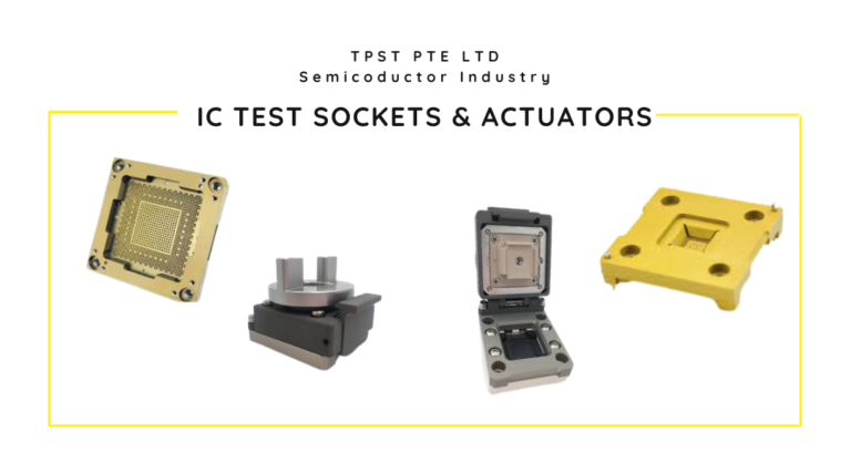
IC Test Sockets and Actuators
- Deal for both handler and hand test
- Supported all device package types like CSP, BGA, QFN, QFP and etc
- Supported all lead counts and package size all lead counts and package size
- Supported minimum pitch 170µm, and low profile minimum test height of 0.5mm
- Minimum Keep out area: approx. 1.5mm beyond the ICs package size
- Customized designs to suit different test function / handler
- Various types of Hand Jig (Lid) to suit to function and cost effectiveness
- Heat dissipation integrated Heat Sink and Fan optio
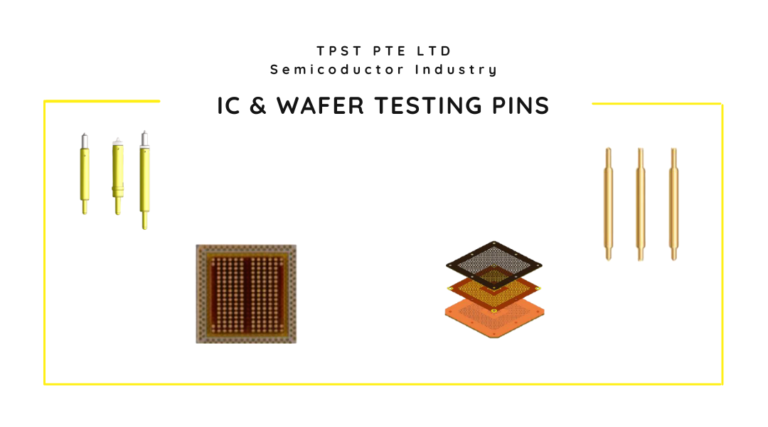
IC & WAFER TESTING PINS
TPST Services Pvt Ltd Provide Standard and customized Pogo pin design with various material type such as Pd alloy, Beryllium Copper, SK4 etc. Diameter down to 0.11 mm.
TPST launched a new silicon rubber socket that can be used to test large surfaced semiconductor packages
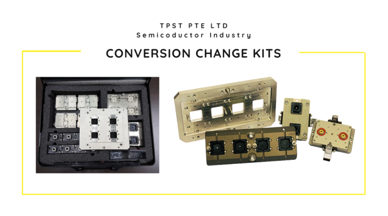
Conversion Change kits
TPST Services Pvt Ltd provides world class High Standard IC Test Sockets for Semicon Industries
TPST Services Pvt Ltd Provide world class Change kit Design and Fabrication of semiconductor conversion kits for major brands of Pick and Place & Gravity feed Test Handlers.
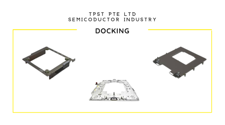
Docking
Reliable docking solution for semiconductor testing.
Our docking plates are adapted to all common handler and prober systems. Integration with our latest advanced technology Manual and Universal types
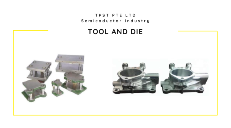
Tool and Die
We provide full range of specialized skills and services to meet customer demand, in serving the Tool & Die needs for the electronics and telecommunications industries. We work closely with customers to develop complete and cost effective integrated service solutions.
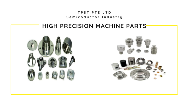
High Precision Machining Parts
TPST Services Pvt Ltd is your one-stop solution for all your precision machining needs. We specialize in CNC-machining of complex medium-size components, in a high-mix low-volume environment